PCB Layers
| Date Published: | |
| Last Modified: |
Soldermask Layer
All values are typical:
- Minimum Solder Mask Sliver = 0.1016mm (4mill)
- Solder Mask Thickness = 11um over copper, 20um over fibreglass (the difference is to that the resulting soldermask surface is flat)
- Common Solder Mask Colours: green (the most common), black, yellow, blue, clear, red and white
- Typical Dielectric Constant: 3-3.3 Note that the darker the solder mask colour (e.g. black), the harder it is to see the copper traces underneath, which in some cases makes it more difficult to debug a faulty PCB. The soldermask colour must be compatible with the silkscreen colour.
Silkscreen Layer
The silkscreen is a printed layer on a PCB which is used to convey information to the user(s) of the board. It usually contains outlines of components, component polarity indicators, component designators, test-point information, and the PCB designer/version. The silkscreen layer(s) helps greatly when manually placing components and soldering the board. The silkscreen is printed on-top of the soldermask, on one or both sides of the board. On really cheap PCB runs, the silkscreen is left-off altogether (because it is not a necessary layer for the board to function). For good readability, it should contrast well with the colour of the soldermask.
Common silkscreen colours are:
| Silkscreen Colour | Relative Cost (out of 5) | Compatible Soldermask Colours |
|---|---|---|
| White | 1 | Green, Red, Black |
| Black | 2 | Green, White, Yellow |
| Red | 4 | White, Yellow |
The silkscreen has to printed on either soldermask or bare PCB, it cannot be printed onto bare or tinned copper. For this reason, you cannot have soldermask on top of component pads.
Components That Protrude Over The Edge Of The PCB
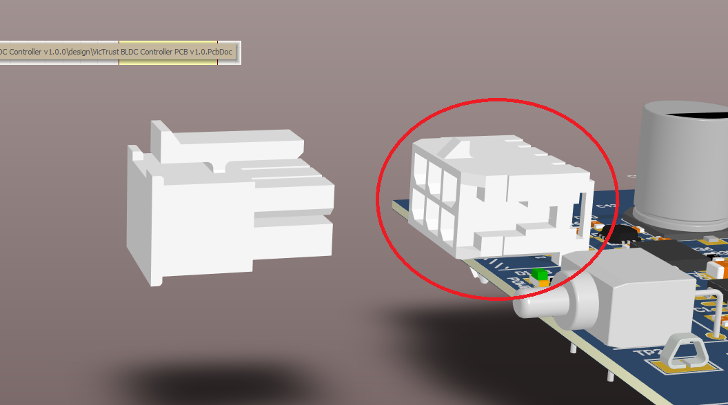
For components that protrude of the edge of the PCB (for example, connectors, or right-angled switches/leds, see the picture above), it is useful to indicate this on the silkscreen layer with diagonal lines as shown in the image below.
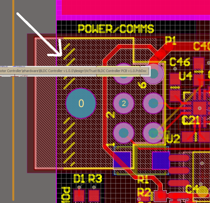
Diagonal lines on the silkscreen layer of a PCB can be useful for indicating a component that protrudes over the edge of a PCB.
For a list of common component designators which are used on the silkscreen layer, see the Component Schematic Symbols and Designators page.
Solder Paste Layer
Solder paste is applied in the PCB manufacturing process just before the board is populated and soldered. It is the way that solder is applied in mass-quantities by a machine, and consists of a powdered metal solder suspended in a thick paste of flux. It is usually passed through a metal stencil which is placed on top of the PCB, which has laser-cut holes in where the paste is to be applied. Since solder paste is only used when the board are to be populated by machine, it is normally not a concern when designing prototypes that will be soldered by hand, and is part of the “design for manufacture” process. For large areas that are going to be covered to solder paste (such as thermal pads on QFN packages), it is recommended that you “window” the stencil, as shown in the image below.
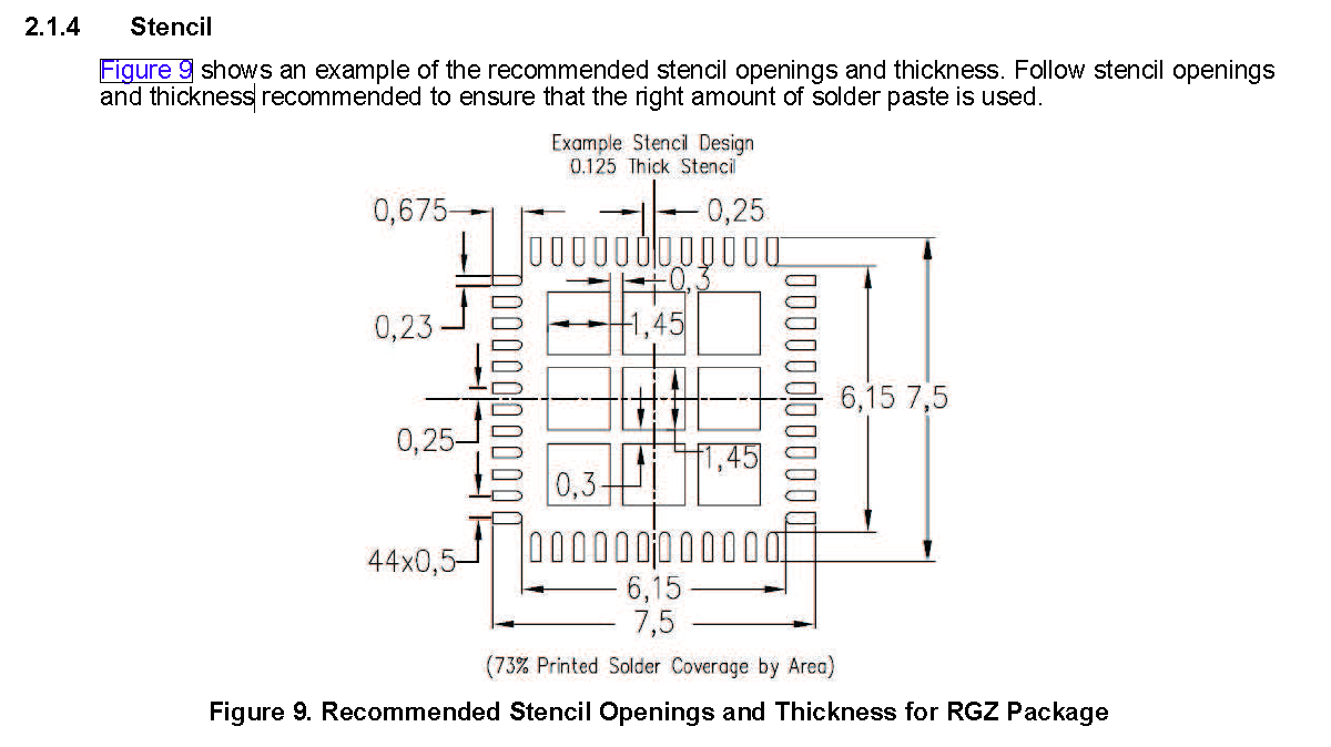
The recommended stencil opening for solder paste on a QFN package. Note the windowing to prevent the package from floating during soldering. Image from http://www.ti.com/lit/an/sloa122/sloa122.pdf.
Authors


This work is licensed under a Creative Commons Attribution 4.0 International License .