General Routing Tips
| Date Published: | |
| Last Modified: |
Overview
See below for PCB routing tips and tricks.
Always Have Schematics In-Front Of You
Having schematics in-front of you when routing is a must. Either print them out or put them on a second monitor if you are lucky enough to have one.
Sometimes it is not obvious from the rats nest to where a component should go. A classic example is decoupling caps. A rats nest will only show one pin connected to the power rail, and the other to ground. However, the schematic show (hopefully!) that it is associated with the power input to an IC, and therefore should be placed next to the IC.
Having the schematic visible also lets you place the components in a logical manner.
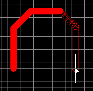
Stress Relief Antennas
Antennas can also be used for stress relief during soldering for stress-sensitive parts, such as accelerometers and gyros. Un-used pins on the stress-sensitive component package are routed a minimum distance from the pad, just like the used pins, so that when soldering using reflow or infrared techniques, all the solder on the pads melts and solidifies at the same time, reducing the stress on the component.
Routing un-used pins on a accelerometer component package a minimum distance away from the IC to reduce stress when infrared/reflow soldering.
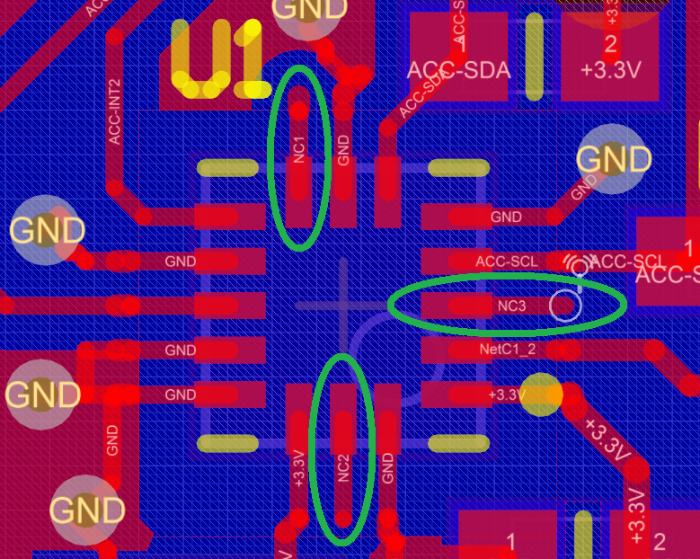
Undesired Antennas
Any PCB antenna that isn’t for radio transmission or stress relief is probably a bad thing. These are cause by tracks end in the middle of nowhere, and are often created un-intentionally when routing the PCB.
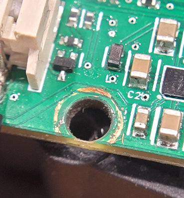
Provide Clearance For Mechanical Screws
Make sure to provide copper (and component) clearance around mechanical screw holes for the screw head. If copper tracks (or planes) are run underneath the screw head, the screw head can bite through the soldermask and do the following:
- Electrically connect itself and whatever the screw is connected to (e.g. a metal enclosure) to a particular net on the PCB.
- Short out two tracks running underneath the screw head.
- Rip tracks of the PCB and make the nets go open circuit.
Authors


This work is licensed under a Creative Commons Attribution 4.0 International License .