TO-Leadless Component Package
| Date Published: | |
| Last Modified: |
Overview
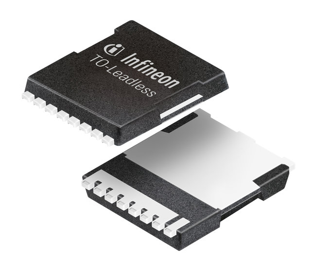
TO-Leadless is a component package is solely used by Infineon for a range of it’s high power MOSFETs1. In this package, Infineon’s MOSFETs can achieve on-resistances as low as 0.4mΩ. It’s package size is 60% smaller than the D2PAK 7-pin package.
The package has 8 leads plus and exposed pad2.
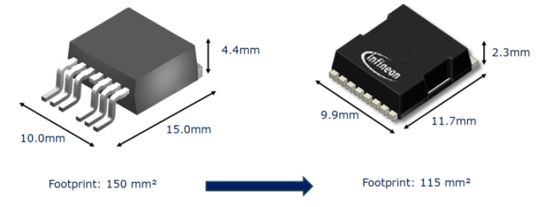
Below is a size comparison between DPAK (left) and TO-Leadless (right):
Synonyms
- PG-HSOF-8: Infineon name2.
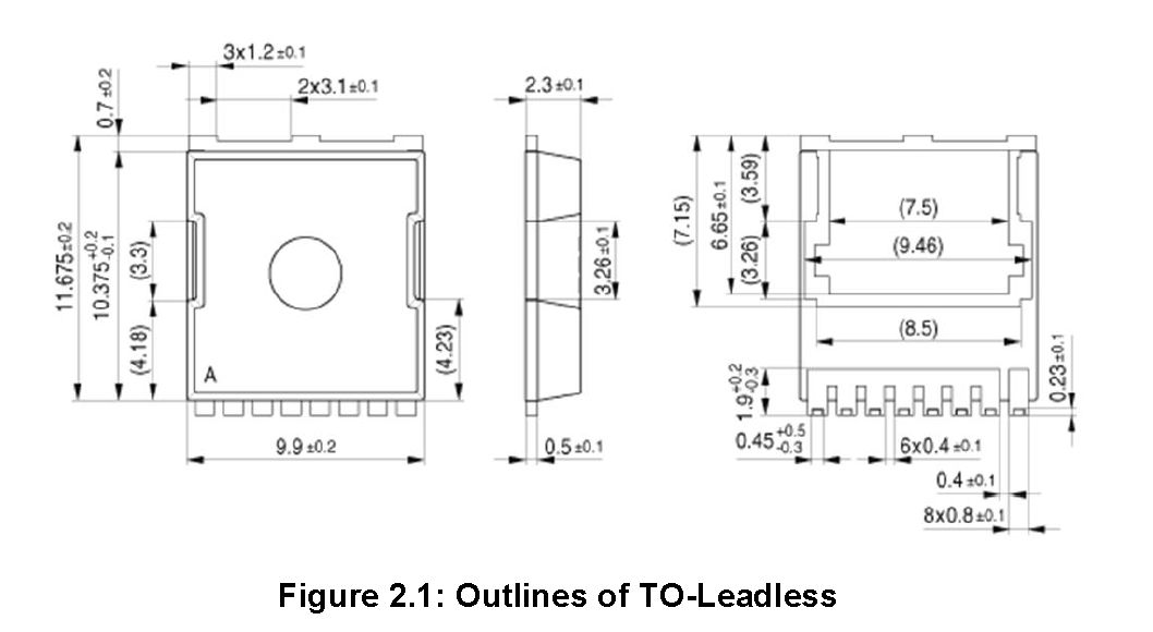
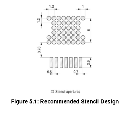
Dimensions
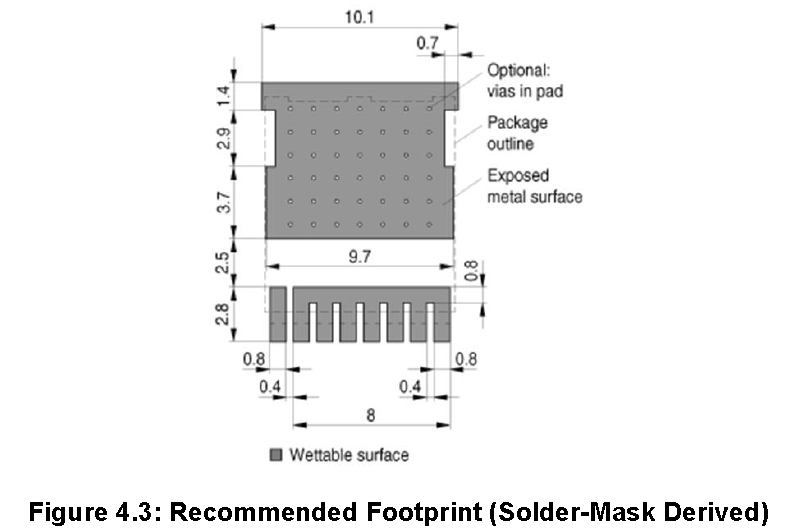
Footprint
Solderability
Not suitable for hand soldering due to pads underneath the package. Suitable for hot air and reflow soldering techniques
Thermal Resistance
- \(R_{JC} = 0.4^{\circ}{\rm C}/W\)
- \(R_{JA} = 40^{\circ}{\rm C}/W\) (max)
References
Infineon. TO-Leadless (TOLL) OptiMOS™ package. Retrieved 2024-04-22, from https://www.infineon.com/cms/en/product/power/mosfet/n-channel/optimos-and-strongirfet-latest-packages/to-leadless/. ↩︎
Infineon. IPT026N10N5 - MOSFET - OptiMOS 5 Power-Transistor, 100V [datasheet]. Retrieved 2024-04-22, from https://www.infineon.com/dgdl/Infineon-IPT026N10N5-DS-v02_01-EN.pdf?fileId=5546d46269e1c019016ac029615332f7. ↩︎ ↩︎
Authors


This work is licensed under a Creative Commons Attribution 4.0 International License .
Related Content:
- TO-5 Component Package
- SOT-762-1 Component Package
- SOT-886 Component Package
- SOT-902 Component Package
- SC-101 Component Package