SOIC Component Package
| Date Published: | |
| Last Modified: |
Overview
SOIC is the name for a family of SMD component packages that have gull-wing leads on two sides of the package. SOIC is a very popular package and is commonly used to house integrated circuits (ICs).
There are are three different widths of SOIC packages, all which can be referred to as just SOIC by manufacturers in component datasheets! When designing a PCB, make sure to double-check the exact package width matches the PCB footprint/land pattern you’ve chosen.
- Package body width of 3.80mm (0.150"). JEDEC standard, commonly used for SOIC packages with a small pin count (16 or less).
- Package body width of 5.30mm (0.208"). EIAJ standard1, used for SOIC packages with higher pin counts (>16) or for isolated ICs (e.g. Maxim package
SOIC [W8]2). - Package body width of 7.52mm (0.300"). JEDEC standard, commonly called SOIC Wide or
SOIC-W(e.g. Maxim packageSOIC (W)variantW20+6)3.
More on these different width SOIC packages below.
Synonyms
- 11-4M1S (Toshiba SO-4, 4.55mm wide body)4
- 751EP (onsemi SOIC4 W5)
- R-PDSO (JEDEC wide body SOIC, 7.5mm width, 0.65mm pitch)
- S8 (SOIC-8, Analog Devices)
- S8E (Linear Technologies, SOIC-8 with exposed pad)
- SO (ST Microelectronics)
- SOIC8E (SOIC-8N with exposed pad, Monolithic Power Solutions6)
- SOT162-1 (SOIC-16W, NXP7)
- SSOP4/LSOP04 (onsemi, SO-4, 7.5mm wide body)8
- WSON (SST, this is a package which shares the same footprint as a SOIC but has a smaller height, not to be confused with the different SON package)
SOIC (JEDEC, 0.150" Package Body Width)
The JEDEC version of the SOIC (a.k.a SOIC-xN (SOIC narrow)) family of packages is governed by the JEDEC MS-012-AA standard. There are non-exposed (normally just referred to as SOIC-x or SOIC-xN) and exposed pad versions (which are normally indicated with an “E” in the package name6).
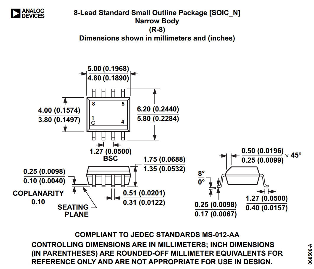
The dimensions for the SOIC-8N package are shown below:
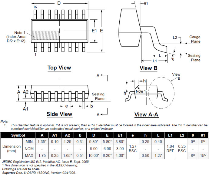
The dimensions for the SOIC-16N component package are shown below:
Land area:
- SOIC-8: 29.4mm2
Thermal resistance:
- SOIC-8: 70.6K/W (pads only, no copper fill)
- SOIC-8: 55K/W (6cm2 of copper, ground pins attached internally to die)
- SOIC-8: 33.5K/W (1 square inch of copper surrounding package, connected to ground)
SOIC (EIAJ, 0.208" Package Body Width)
Confusingly, the EIAJ standard defines a different body width of 5.3mm (0.208") for the `SOIC`` package, compared to the 3.8mm body width as defined in the JEDEC standard1. Generally used for ICs with a larger number of pins (>16).
SOIC-W (JEDEC, 0.300" Package Body Width)
The SOIC-W (SOIC wide) family of packages is governed by the JEDEC MS-013 and IEC 075E03 standards. NXP’s SOT-162-1 package is a SOIC-16W7.
| Package Name | Land Area |
|---|---|
| SOIC-16W | 136.3mm² (11.9x11.45mm)7 |
| SOIC-28W | 186.4mm² (10.3x18.1mm) |
Pitch
Most SOIC packages have a pitch of 1.27mm (50mil) and usually have Gullwing leads. When used for regulators, sometimes the many ground pins are connected internally to the die attach flag, providing better heat sinking capabilities. SOIC packages use leadframe technology.
The SOIC package R-PDSO defined by JEDEC has a non-standard pitch of 0.65mm (and the standard wide body width of 7.5mm).
Pin Numbering
Pin numbering is the same as a DIP package, in that pin 1 is at the top left, and then pins are numbered sequentially down the left-hand side, then up the right hand-side.
Polarity Marks
There are three ways of indicating the polarity on a SOIC package. The first two, a dot or a notch, indicate pin 1 or the top of the chip. The third way is not so obvious, and features a bevelled edge along the side that pin 1 is on (so for SOIC-8, the bevelled edge would be on the side with pins 1 to 4).
Related Packages
The WSON package by SST is lower in height than a standard SOIC package, but is designed to use the same PCB footprint.
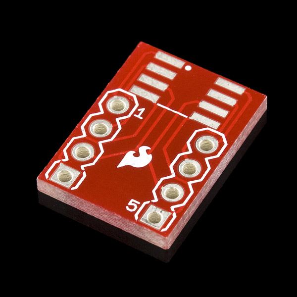
Adapter PCBs
Adapter PCBs for the SOIC family of packages are widely available due to the popularity of the package.
SparkFun makes a SOIC-8 to DIP-8-300 adapter PCB.
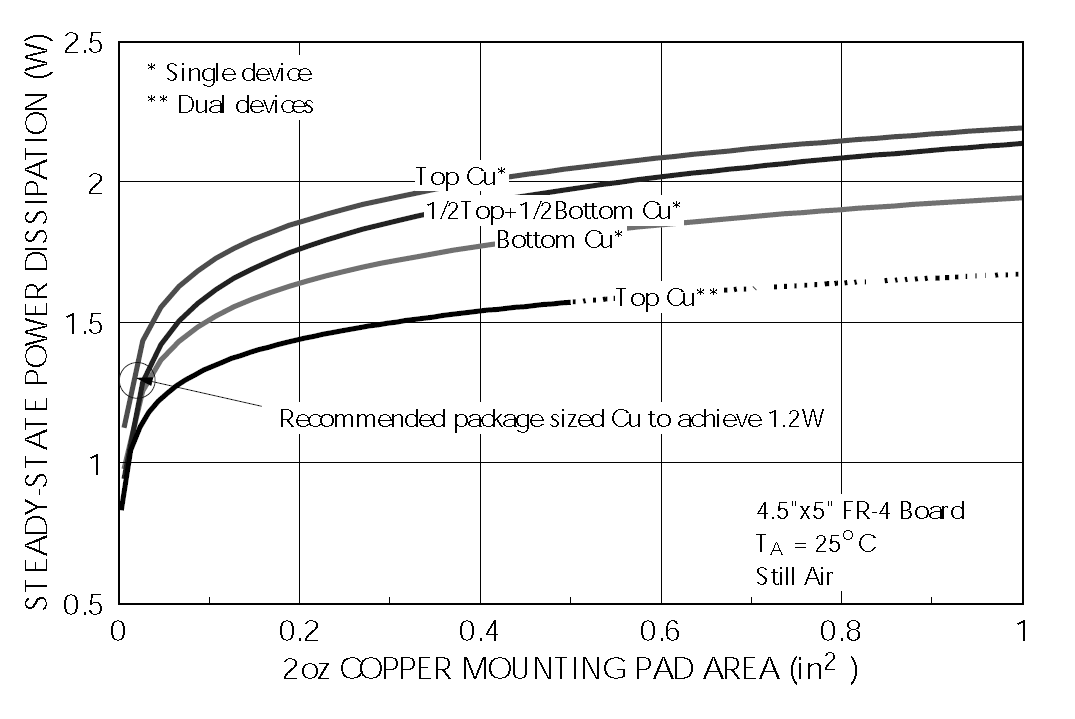
Thermal Resistance And Power Dissipation
This graph shows the maximum power dissipation for the SOIC-8N component package, for various PCB copper areas.
Standard Pinout For MOSFETs
The SOIC-8 component package is commonly used for medium-power N and P-channel MOSFETs. Most of these MOSFETs have the exact same pinout (both N and P-Channels!), as shown in the below diagram.
As far I’m aware, this is not specified in any standard, but is just an industry default. Also, this only applies to SOIC-8 packages with 1 MOSFET inside them.
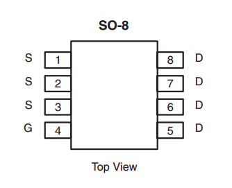
Examples that follow this pinout include the ST STS25NH3LL (N-channel), the International Rectifier IRF8721PbF-1 (N-channel), and the Vishay SI9407BDY-T1-GE3 (P-channel).
SOIC-4 (SO-4)
The SO-4 package is quite unique from other SO packages. It typically has the same mechanical dimensions as a SO-6 package, but has the two middle pins on either side removed. Typically the SO-6 pin numbering is also kept, such that the remaining pins are numbered 1, 3, 4 and 6. Due to the large clearances between the pins and on the package, this SO-4 package is used for optical isolators.
The SO-4 package is different to the SOIC-4 package, even though these two different names refer to the same package at higher pin counts.
ON Semiconductor uses the case code 751EP for the SOIC-4W package5.
Common Uses
- Linear regulators.
- Drivers/buffers.
- High-power MOSFETs (normally in a SOIC-8N, with one pin for the gate, and either 3 or 4 pins for the drain and source).
Similar To
- QFP: Another SMD package used for ICs with gull-wing leads (QFP has leads on all four sides of the body).
- SOJ: Similar body sizes to SOIC, but with J-type leads instead of gull-wing leads.
References
DEX PCB. Device Overview > SOIC. Retrieved 2022-03-08, from https://dexpcb.com/manual/device_overview.htm. ↩︎ ↩︎
Maxim. Package Land Pattern: [W8] 0.208" SOIC, 8 Leads. Retrieved 2022-03-08, from https://pdfserv.maximintegrated.com/land_patterns/90-0258.PDF. ↩︎
Maxim (2013, Jan 17). Package Outline: 20L, 28L SOIC .300". Retrieved 2022-03-08, from https://pdfserv.maximintegrated.com/package_dwgs/21-0703.PDF. ↩︎
Retrieved 2021-12-08, from https://media.digikey.com/pdf/Data%20Sheets/Toshiba%20PDFs/TLP185_04-27-17.pdf. ↩︎
On Semiconductor (now onsemi) (2019, Sep). Bridge Rectifiers, 0.5 A: MB10S (datasheet). Retrieved 2022-03-08, from https://www.mouser.com/datasheet/2/308/1/MB10S_D-2314909.pdf. ↩︎ ↩︎
Monolithic Power Solutions (2012, May 30). MP2497-A: 3A, 50V, 100kHz Step-Down Converter with Programmable Output OVP Threshold. Retrieved 2022-01-20 from https://www.monolithicpower.com/en/documentview/productdocument/index/version/2/document_type/Datasheet/lang/en/sku/MP2497A/document_id/1972. ↩︎ ↩︎
NXP (2016, Feb 8). SOT162-1: Plastic small outline package; 16 leads; body width 7.5 mm (package information). Retrieved 2022-01-25, from https://www.nxp.com/docs/en/package-information/SOT162-1.pdf. ↩︎ ↩︎ ↩︎
Retrieved 2021-12-08, from https://nz.mouser.com/datasheet/2/308/1/FODM1009_D-2313636.pdf. ↩︎
Authors


This work is licensed under a Creative Commons Attribution 4.0 International License .
Related Content:
- SC-101 Component Package
- SMD-220 Component Package
- TO-5 Component Package
- PP3 Component Package
- SIM Card Sizes