LGA Component Package
| Date Published: | |
| Last Modified: |
Overview
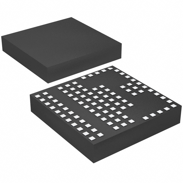
The LGA package is is a surface mount package with pads on the underside of the package. It is very similar to the BGA package, except is does not have any balls, instead plain flat pads are used. An LGA package may also differ from BGA with the addition of arbitrary sized pads for purposes such as grounding, thermal dissipation, shielding and mechanical strength. An LGA package can be made from a PCB, thus many LGA components are actually entire “modules” made from a PCB and a number of components. This modular form is commonly seen with cellular modem and WiFi components.
CPU Variants:
| Code | Socket Name |
|---|---|
| LGA 771 | Intel Socket J |
| LGA 775 | Intel Socket T |
| LGA 1150 | Intel Socket H3 |
| LGA 1155 | Intel Socket H2 |
| LGA 1156 | Intel Socket H |
| LGA 1207 | AMD Socket F, AMD Socket C32 |
| LGA 1356 | Intel Socket B2 |
| LGA 1366 | Intel Socket B |
| LGA 1944 | AMD Socket G34 |
| LGA 2011 | Intel Socket R |
The LGA package comes in many different variants, all which have a different number of pins and a different pin configuration. The pins are normally lines up in a grid of x columns and y rows, but not every position may have a pad. Therefore you can get variants with the same LGA package width and length.
Cannot solder with a soldering iron, soldering with hot air or infrared is o.k., recommended practise is to use reflow techniques.
Like BGAs, LGA packages can withstand up to 50% mis-alignment when soldering (50% of the distance between consecutive pads, i.e. it’s pitch), as the package will automatically align itself1. LGA packages can be connected to the PCB either with a socket or direct soldering. Intel has popularised the package by using it on some of it’s CPU families.
Socket
Shifted Solder Mask Layouts
Sometimes LGA components recommend unique paste mask designs with “shifted” openings, as shown below.
![The recommended paste mask layout (Panasonic labels this the "solder mask", but they are really talking about what most people call the paste mask!) for the Panasonic PAN9026. Notice the unequal shifting of approx. 150um[^bib-panasonic-pan9026-design-guide].](https://blog.mbedded.ninja/pcb-design/component-packages/lga-component-package/_assets/panasonic-pan9026-solder-mask-layout.png)
The recommended paste mask layout (Panasonic labels this the “solder mask”, but they are really talking about what most people call the paste mask!) for the Panasonic PAN9026. Notice the unequal shifting of approx. 150um2.
Common Uses
- CPUs
- Cellular modems
- WiFi modules
Similar To
- BGA: A BGA has balls on the underside pads, while a LGA doesn’t.
- PGA
References
NXP (2009, Oct). AN3241: Land Grid Array (LGA) Package Rework. Retrieved 2022-04-19, from https://www.nxp.com/docs/en/application-note/AN3241.pdf. ↩︎
Panasonic. PAN9026: Wi-Fi Dual Band 2.4/5 GHz and Bluetooth Module. Design Guide. Rev. 1.1.. Retrieved 2022-04-19, from https://mediap.industry.panasonic.eu/assets/custom-upload/Devices/Wireless%20Connectivity/Wi-Fi%20Modules/PAN9026/WM%20PAN9026%20Design%20Guide.pdf. ↩︎
Authors


This work is licensed under a Creative Commons Attribution 4.0 International License .
Related Content:
- SC-101 Component Package
- SMD-220 Component Package
- TO-5 Component Package
- PP3 Component Package
- SIM Card Sizes