Bipolar Junction Transistors (BJTs)
| Date Published: | |
| Last Modified: |
Overview
Bipolar junction transistors (BJTs) are 3 legged active electrical semiconductor components. They behave as a current-amplifier, amplifying a small base-emitter (BE) current into a larger collector-emitter (CE) current.
BJT transistors were the second type of transistor to be mass produced (superseding the Type-A transistor), at the first at very large quantities1.
They are used for making things such as amplifiers, switches, linear regulators, current mirrors and digital logic.
Types
BJTs come in two flavours, NPN or PNP. They both have three terminals, the collector (C), the base (B) and the emitter (E).
The differences between the NPN and PNP transistor types are analogous to the N-Channel and P-Channel MOSFET types.
Schematic Symbols
The schematic symbols for NPN and PNP transistors are shown below:
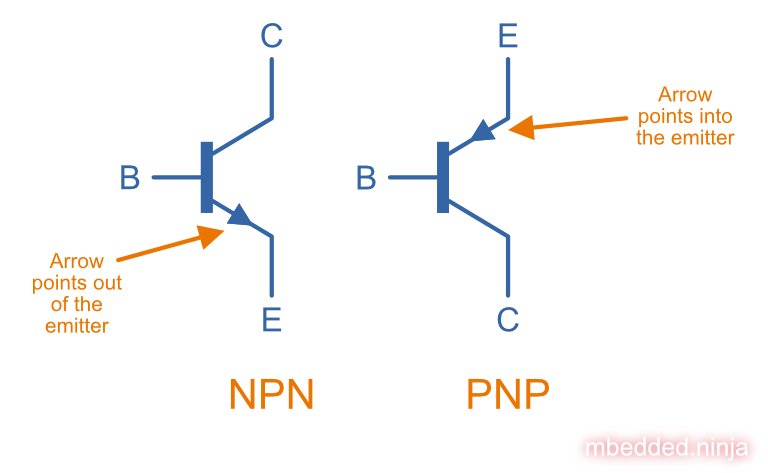
Schematics symbols for NPN and PNP transistors. Note that the collector and emitter have flipped positions for the PNP, as commonly drawn on schematics.
Notice that the collector and emitter have been flipped for the PNP (compared to the NPN), this is how they are normally drawn on schematics.
The arrow is always on the emitter leg of the BJT. To differentiate between the two, the arrow on the NPN points away from the transistor, the arrow on a PNP points towards the transistor.
Sometimes you will see the transistors drawn without the circles around them, they represent exactly the same thing as the symbols above.
How They Work
BJTs are made from a hunk of silicon. They are either a thin slice of P-type semiconductor sandwiched between two layers of N-type semiconductor (NPN) or the reverse, a thin slice of N-type semiconductor sandwiched between two layers of P-type semiconductor (PNP).
The bipolar part of their name comes from the fact they conduct by using both majority and minority charge carriers.
BJT Characteristics
BJT characteristics is a family of curves that show you how a BJT responds to various currents and voltages across it’s terminals. Normally two parameters are varied whilst a third is held constant. BJT characteristics can be broken down into:
- Input characteristics: How \(I_{B}\) changes with \(V_{BE}\), at constant \(V_{CE}\)2.
- Transfer characteristics: How \(I_C\) changes with \(I_B\), at constant \(V_{CE}\).
- Output characteristics: How \(I_C\) changes with \(V_{CE}\), at constant \(I_B\).
- Mutual characteristics: How \(I_C\) changes with \(V_{BE}\)3.
Output Characteristics
The characteristic output curve for a BJT shows show the collector current \(I_C\) changes as the collector-emitter voltage \(V_{CE}\) changes, at a fixed base current \(I_B\). This curve is shown for a number of base currents to cover a range of operation points, and generally you can interpolate between the curves for your specific base current if needed.
The below figure shows the simulated output transfer characteristics for the popular 2N2222 BJT. \(I_C\) is plotted against \(V_{CE}\) for a range of base currents \(I_B\) varying from 0 to 5mA:
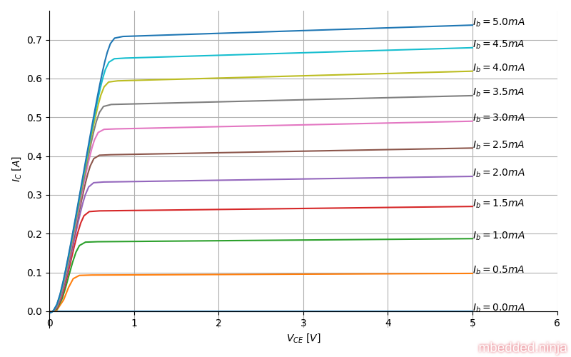
(Micro-Cap simulation file: circuit.cir)
Important Parameters
Beta And Gain (B, hfe)
The gain of a BJT is the ratio between the base current and the collector current (hence it is a current gain), typically when measured with the BJT in a common-emitter configuration. There are few different gains and symbols used, so it’s important to know what exact gain is being talked about:
- \(\beta\): DC (large-signal) gain
- \(H_{fe}\) (or \(h_{FE}\)): DC (large-signal) gain, part of the H-parameter (Hybrid parameter) model (same as \(\beta\)). Also sometimes written as \(h_{21}\)
- \(h_{fe}\): Small-signal gain, part of the H-parameter model
All of them depend somewhat other parameters such as collector current and temperature, but typically the gain is treated as a constant. The main thing to remember is to not expect the current gain to equal an exact number, even between the same BJT transistor from the same manufacturing batch.
$$\begin{align} I_C = \beta I_B \end{align}$$The \(FE\) part of the two H-parameter gains represents:
- \(F\): The Forward current amplification
- \(E\): As measured with the BJT in the common-Emitter configuration
Temperature has a major influence on the gain of a BJT.
Early Voltage (Va)
- Symbol: \(V_A\)
The Early Voltage is a parameter used to determine the Early effect. The Early effect describes the small increase in collector current as the collector-emitter voltage increases (with a BJT operating in it’s saturation region). As \(V_{CE}\) on a BJT increases, the reverse-bias on the \(V_{CB}\) junction increases (this is just a PN junction in reverse bias under typical operation). This increases the depletion region of this junction, which reduces the effective width of the base. Because the saturation current is inversely proportional to the effective width of the base, an increase in \(V_{CE}\) results in an increase in \(I_C\).
The effect of the collector-emitter voltage on collector current is given by the following equation:
$$\begin{align} I_C = I_{C(sat)} ( 1 + \frac{V_{CE}}{V_A} ) \end{align}$$where:\(V_A\) is the Early voltage
The Early voltage can be derived from \(I_C\) vs. \(V_{CE}\) graphs. If you extrapolate the active part of the curve (beyond the knee) back to where the line crosses the x-axis, this gives you the negative of the Early voltage, \(-V_A\). It should not matter what the base current \(I_B\) is, all the curves should cross the x-axis at the same point. The following graph shows this:
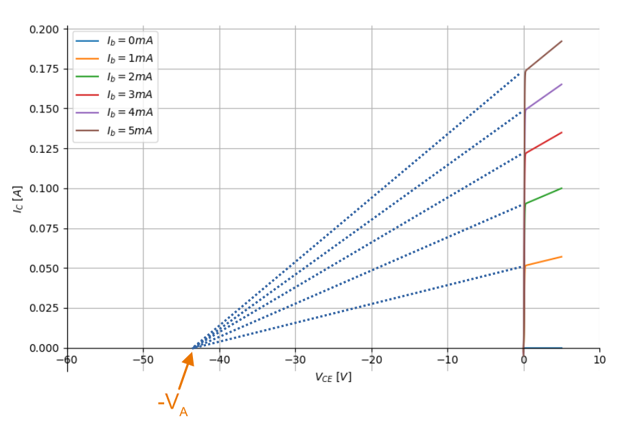
Graph of Vce vs. Ic showing how the Early voltage is the extrapolation of the curves (in the active region) back to the x-axis intersection.
(Micro-Cap simulation file: early-voltage.cir)
Micro-Cap with the QNB transistor was used to simulate these \(I_C\) vs. \(V_{CE}\) curves. This model had a Early voltage VAF set to 45V, which agrees well with the extrapolated curves and the x-axis intersection.
In SPICE models, the variable VAF is typically used to denote the Early voltage (standing for forward Early voltage).
Miller Capacitance
TODO: Add notes here
Thermal Voltage
The thermal voltage of a BJT transistor is the voltage across a PN junction caused by the temperature of the junction.
$$\begin{align} V_T = \frac{kT}{q} \end{align}$$where:\(k\) is Boltzmann's constant in Joules per Kelvin, which is \(1.38\times 10^{-23}JK^{-1}\)\(T\) is the temperature of the junction, in Kelvin \(K\)\(q\) is the charge on a electron in Coulombs, which is \(1.6\times 10^{-19}C\)
At a room temperature of \(22^{\circ}C\), \(V_T\) is approximately \(25mV\). \(25mV\) is a good enough approximation for the thermal voltage in many scenarios without taking the actual junction temperature into account. The thermal voltage is used in the hybrid-pi model of the BJT transistor.
BJT Transistor Models
Ebers-Moll Transistor Model
TODO: Add info here
Hybrid-Pi Transistor Model
The hybrid-pi model is a well-used model for approximating the small-signal behaviour of transistors at low frequencies. There are a few variants of the hybrid-pi model, the simplest being the small-signal linearized version. It is also known as the Giacoletto model after L.J. Giacoletto who designed it in 19694.
Small-Signal Linearized Hybrid-Pi Model
The small-signal linearized hybrid-pi model is a simplification of the complete hybrid-pi model.
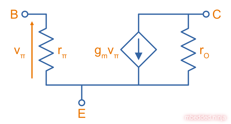
Inputs (independent variables) to the model are:
- Small-signal base-emitter voltage \(v_\pi\)
- Small-signal collector-emitter voltage \(v_{CE}\)
From this the model calculates the following outputs (dependent variables):
- Small-signal base current \(i_B\)
- Small-signal collector current \(i_C\)
The transconductance \(g_m\) can be calculated with (evaluated when \(v_{ce} = 0\))4:
$$\begin{align} g_m &= \left. \frac{i_C}{v_{BE}} \right|_{v_{ce}=0} \nonumber \\ \label{eq:gm-ic-vt} &= \frac{I_C}{V_T} \\ \end{align}$$where:\(I_C\) is the DC bias collector current (not the small-signal collector current)\(V_T\) is the thermal voltage (see above for more info on this)
The resistance between the base and emitter as looking into the base, \(r_{\pi}\), is equal to4:
$$\begin{align} r_{\pi} &= \left. \frac{v_b}{i_{be}}\right|_{v_{ce}=0} \nonumber \\ \label{eq:rpi-vt-ib} &= \frac{V_T}{I_B} \\ \end{align}$$Why do we specify “as looking into the base” when specifying the resistance between base and emitter? Surely it’s the same “as looking into the emitter”? For a two terminal component such as a basic resistor, this would be true. But for a three terminal component such as a BJT, the current going into the base is not the same as the current coming out of the emitter. So when calculating the apparent resistance, even though the voltage between base-and-emitter is the same, the current depends on whether you are “looking into” the base or the emitter.
By using \(h_{fe} = \frac{I_C}{I_B}\) and \(Eq. \ref{eq:gm-ic-vt}\) we can substitute into \(Eq. \ref{eq:rpi-vt-ib}\) to re-write \(r_{\pi}\):
$$\begin{align} r_{\pi} &= \frac{h_{fe}}{g_m} \\ \end{align}$$The output resistance, \(r_O\), can be found with4:
$$\begin{align} r_{O} &= \left. \frac{v_{ce}}{i_c} \right|_{v_{be}=0} \nonumber \\ &= \frac{1}{I_C}(V_A + V_{CE}) \nonumber \\ &\approx \frac{V_A}{I_C} \\ \end{align}$$Circuit Design Basics With BJTs
The current through the base pin (\(I_b\)) and the current through the collector pin (\(I_c\)) always sums to give the current through the emitter pin (\(I_e\)).
$$\begin{align} I_e = I_b + I_c \end{align}$$Because the collector current is usually much larger than the base current, for most scenarios you can treat the collector and emitter current as equal.
$$\begin{align} I_e \approx I_c \end{align}$$As a general rule, NPN transistors are useful for connecting things to ground. PNP transistors are useful for connecting things to your power rail.
NPNs require a small positive base-emitter voltage to create a current which flows into the base. This current, multiplied by the gain of the transistor, determines the collector-to-emitter current (well, to be technically correct, the maximum collector current). Because of this, a NPN transistor will only conduct when both the base and collector have a higher voltage than the emitter.
A PNP transistor will only conduct when both the base and collector have a negative voltage w.r.t the emitter.
High And Low-side Switching With BJTs
NPN transistors are good for low-side switching. You can connect the collector to the negative end of the load, the emitter to ground, and control the base with a digital low/high signal through a resistor (low/ground base signal = load off, high base signal = load on).
However, NPN transistors cannot be used as a simple high-side switch, as the emitter rises to the high-side load voltage. To keep the NPN transistor in saturation, this would mean the base voltage would need to be higher than the high-side load voltage, which is not usually viable (charge-pumps are sometimes used to overcome this, but more commonly seen when using N-channel MOSFETs as high-side switches). Normally you would want to use a PNP transistor for high-side switching.
BJT Circuits
Common-Base Amplifier
The BJT common-base (a.k.a. grounded-base, and sometimes just abbreviated to CB or GB) amplifier is one of the three basic single-stage BJT amplifier topologies. The base of the BJT is connected to ground and shared with the output signal, hence the “common-base”. The input signal is fed to the emitter and the output comes from the collector. It is not as popular in discrete low-frequency circuits as the common-collector or common-emitter BJT amplifiers.
A basic schematic of a common-base NPN BJT amplifier is shown below, excluding DC biasing components:
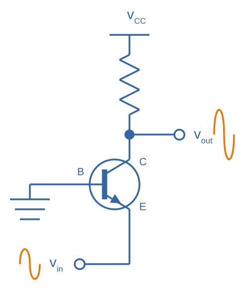
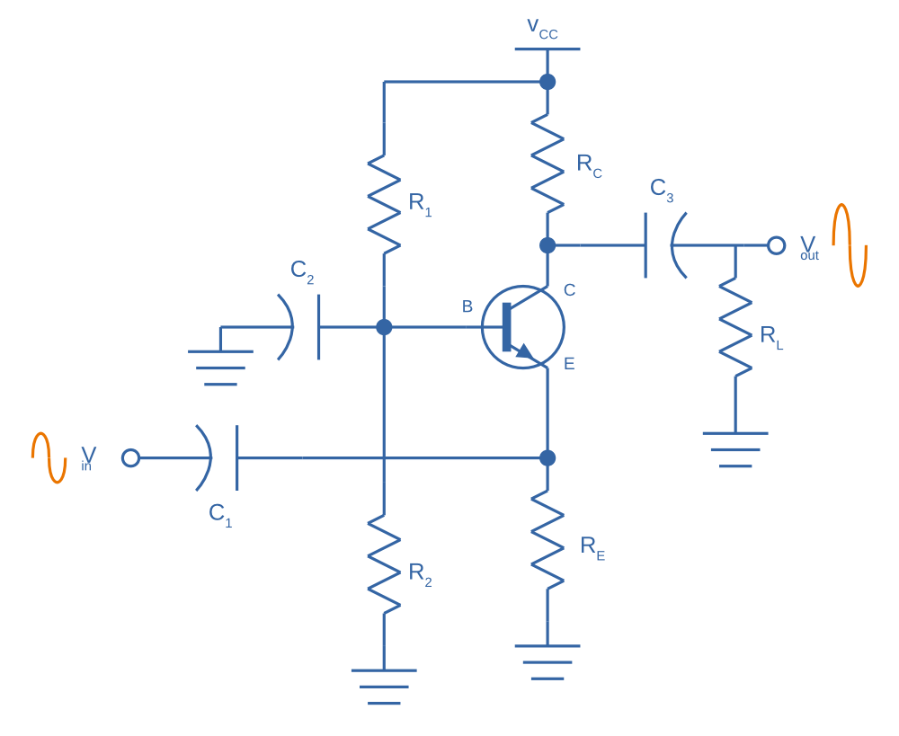
Note that the above circuit is not realistic because it does not show the DC biasing componentry, however it is useful to illustrate the basic principle of the amplifier. The following schematic shows a common-base amplifier with the DC biasing component included:
Input Resistance
The small-signal input resistance of the common-base BJT amplifier is equal to:
$$\begin{align} r_{in} &= \frac{v_{in}}{i_{in}} \\ &= \frac{v_e}{i_e} \\ &= \frac{i_e \cdot (r'e\,||\,R_E)}{i_e} &\text{Replacing $v_e$} \\ &= r'e\,||\,R_E &\text{$i_e$'s cancel out} \end{align}$$Basic BJT Amplifier Topology Summary
| Topology | Voltage Gain (AV) | Current Gain (AI) | Input Resistance | Output Resistance |
|---|---|---|---|---|
| Common-emitter | Moderate (-Rc/Re) | Moderate (B) | High | High |
| Common-collector | Low (approx. 1) | Moderate (B + 1) | High | Low |
| Common-base | High | Low | Low | High |
Constant-Current Sink
BJTs can be configured to sink a relatively constant amount of current which is independent on the output-side voltage. This can be a useful way of driving an LED from a microcontroller with a constant current, no matter what voltage source is used to drive the LED. BJT current sinks and sources are good for simple, cheap situations in where high precision is not the name of the game. If you want high precision, you’re best bet is to build a current-sink from an op-amp.
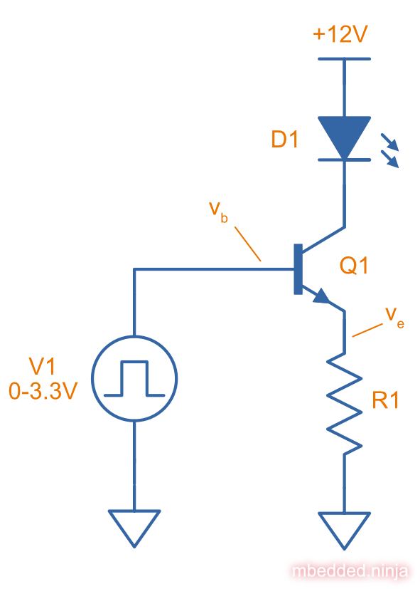
The schematic above was designed to drive the LED with 10mA of current when the BJT was driven from a microcontroller running at \(+3.3V\). Since \(+3.3V\) is applied to the base of the NPN transistor, the transistor will always turn on just enough so that the voltage at the emitter is \(0.7V\) less, e.g.
$$\begin{align} V_e = V_b - 0.7V \end{align}$$Since we know the emitter voltage is going to be \(+2.6V\), we can choose the right resistor, \(R_1\) to get the LED current we desire (remember that the current out of the emitter is pretty much equal to the current into the collector).
$$\begin{align} R_1 = \frac{V_e}{I_{LED}} \end{align}$$So if we want a LED current of 10mA, that means we need \(R1 = 260\Omega\). The closest E12 value is \(270\Omega\).
Notice how the LED current is independent of the \(+12V\). The \(+12V\) can change to say, \(+9V\) and the LED current will still be \(10mA\). The current draw from the microcontroller into the base of the transistor will be very low (somewhere around \(100uA\)).
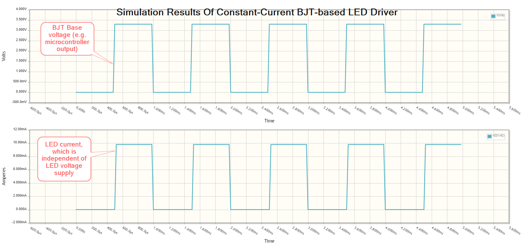
Below are the simulation results for the schematic above, showing the LED current to be indeed \(10mA\). It works!
[[constant-current-bjt-based-led-driver-simulation-results]]
Using A Resistor Divider To Drive The Base
A resistor divider can simple way to drive the base of an NPN current-sink if you don’t need active control. This works well if the supply voltage is known and stable, as the current will fluctuate with supply voltage (if this is going to be an issue, consider using a Zener-based circuit to drive the base of the NPN BJT). Schematics of the design are shown below.
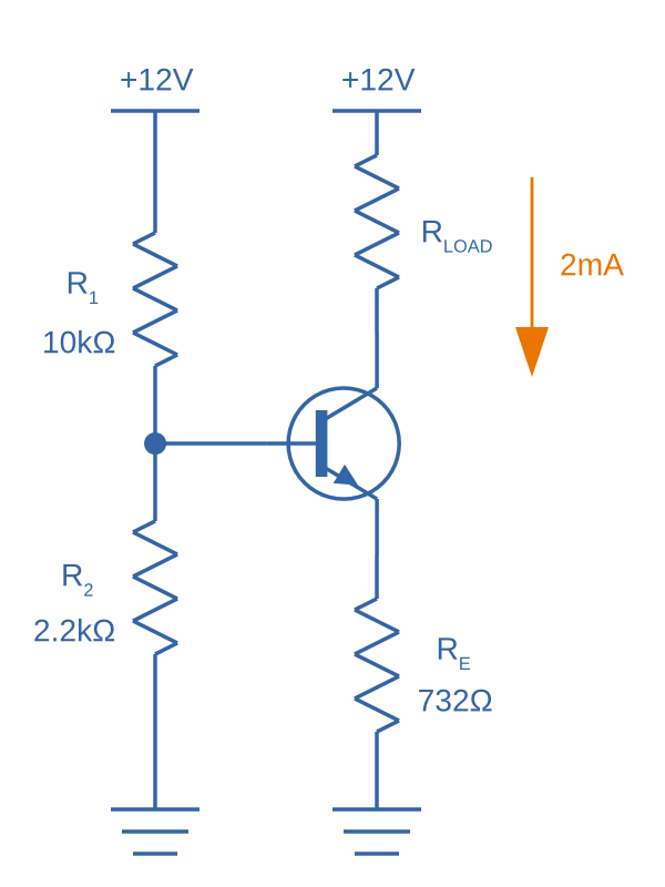
Design Procedure:
Choose the resistor-divider \(R_1\) and \(R_2\) to provide a voltage at the base of the transistor in the region of \(2.0-5.0\)V. I choose \(R_1 = 10k\Omega\) as this is a standard resistance, and then \(R_2 = 2.2k\Omega\) to give a \(V_B = 2.16V\). This uses the standard resistance divider rule, which assume negligible current is drawn from the resistor divider through the base of the transistor.
Subtract \(0.7V\) of \(V_B\) to get \(V_E\). In this case, \(V_E = 1.46V\).
Size \(R_E\) to set the desired current of your current sink. Using Ohm’s Law, \(R_E = \frac{V_E}{I}\). In this case we wanted \(2mA\) to drive an LED, so:
$$\begin{align} R_E &= \frac{1.46V}{2mA} \nonumber \\ &= 730\Omega \nonumber \\ &= \approx 732 \, \text{(closest E96 value)} \end{align}$$As a sanity check, make sure the output impedance of the resistor divider is much less than the input impedance looking into the base of the BJT (otherwise the resistor divider output will get significantly loaded and it’s output voltage will drop). That is:
$$\begin{align} R_1 || R_2 &\ll \beta R_E \nonumber \\ \frac{10k\Omega \cdot 2.2k\Omega}{10k\Omega + 2.2k\Omega} &\ll 100 \cdot 732\Omega \nonumber \\ 1.80k\Omega &\ll 73.2k\Omega \end{align}$$The above equation holds true so this design should work as a good current sink ✅
Current Mirrors
A current mirror is a current-copying circuit in where one the current in one BJT is programmed via a resistor and is used to control the current in a second BJT which is used to drive the same current into a load. The current-mirrors shown below are built with BJTs, but other active transistors such as MOSFETs can also be used. The below image shows a basic PNP BJT-based current mirror.
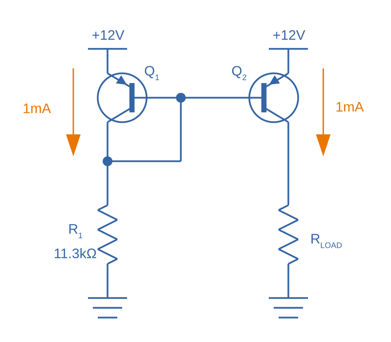
A basic PNP-based current mirror programmed to source 1mA into the load. Q1 and Q2 should be a matched transistor pair to achieve good mirroring of the current.
Design Procedure:
Decide on the program current, \(I_P\). This will also be the current through the load. We’ll use this value later! For this example we’ll choose \(1mA\).
Find the voltage across \(R_1\), nothing that \(Q_1\) has a diode voltage drop of \(0.7V\) from emitter to base (with the emitter tied to \(V_{CC}\)), at that the base and collector of \(Q_1\) are tied together and hence at the same voltage:
$$\begin{align} V_{R1} &= 12V - 0.7V \nonumber \\ &= 11.3V \end{align}$$Set the resistance of \(R_1\) using Ohm’s Law:
$$\begin{align} R_1 &= \frac{V_{R1}}{I_P} \nonumber \\ &= \frac{11.3V}{1mA} \nonumber \\ &= 11.3k\Omega \end{align}$$All done!
For more info, see the Current Mirrors page.
Capacitance Multipliers
Go to the Capacitance Multipliers section to see how BJT transistors are used in capacitance multipliers.
Common BJTs
2N2222
The 2N2222 was first introduced by Motorola at the 1962 IRE convention (using a novel new STAR technology)5. Since then the 2N2222 has been made by a number of different manufacturers. Complementary pair to the PNP 2N2907.
BC547/548/549
The BC range of BJTs, including the BC547 and BC548 are very common, low-cost general purpose BJT transistors that you will encounter in hobbyist and professional electronics designs alike. They originated with the BC108 family of metal-cased transistors.
BC547: Same as the BC548 (NPN), but with a higher breakdown voltage.BC548: Common NPN transistor, used for switching and amplification purposes. Suitable replacement for the2N2222as long as max. voltage/current rating are not exceeded.BC549: Low noise version of the BC548.
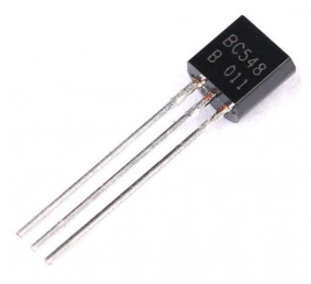
A photo of the ubiquitous BC548 BJT transistor in to TO-92 package. Image from https://www.dnatechindia.com/bc-548-npn-transistor-buy-online-india.html.
S8050/S8550
The S8050 is a popular NPN BJT made by a number of manufacturers. Most versions generally have \(I_C\) of \(700mA\) and a \(V_{CE}\) of \(20V\)6. \(h_{FE}\) can vary from approx. \(120\) to around \(300\) depending on the suffix code. The S8050 is normally found in the TO-92-3 case.
The S8550 is the complementary PNP transistor7.
Multiple-Collector And Multiple-Emitter BJTs
Multiple emitter and multiple collector BJTs are special types of BJTs which have more than one emitter or more than one collector.
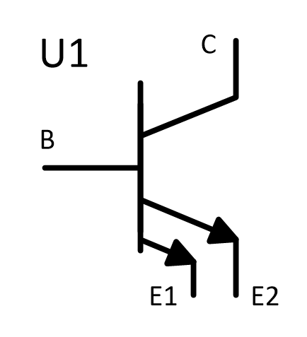
In the case of a multiple collector BJT, the total collector current \(I_{C,tot}\,\) is set by the base current \(I_B\). If all the collectors are the same size (the silicon is physically the same size), then the current is equally split across all collectors.
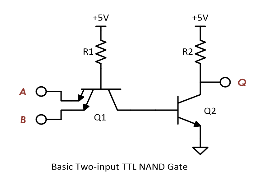
The multiple-emitter BJT can be used to implement AND logic. The multiple-emitter BJT forms an integral part of the TTL AND input circuitry (e.g. the 7400 series of integrated circuits). They were introduced into digital logic design to replace the diodes of diode-transistor logic (DTL), with the advantage of a lower switching time and lower power dissipation.
Multiple emitter BJTs were also used in older (e.g. from the 1960’s) RAM. For example, Intel’s first IC, the 3101 (64 bits of RAM!), contains multiple emitter BJTs as part of the 2-state latch circuitry which holds one bit of information. One emitter is used to select which cell to read or write, while the other emitter is used to read or write the data. See an excellent tear-down of the IC on Ken Shirriff’s blog.
Reverse Active Mode
By utilizing the voltage regulation hysteresis behaviour of a BJT in reverse active mode, it can be used to create a simple single transistor LED blinker
The BJT Safe Operating Area
The safe operating area of a BJT defines the region of voltage and current in which the BJT can be operating in safely without causing damage. It is usually determined by the following limits:
- Maximum collector current
- Maximum collector-emitter voltage
- Maximum power dissipation
- [^What Is Second Breakdown?, Secondary breakdown] (only applicable to power BJTs)
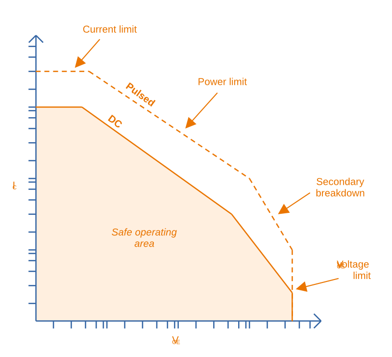
A typical representation of the safe operating area (SOA) of a BJT. Normally multiple curves are drawn, one for DC and a number for pulses of various lengths. Both \(V_{CE}\) and \(I_C\) are on logarithmic axes.
What Is Second Breakdown?
Second breakdown (a.k.a second breakdown) is a limitation on the SOA that is typically only an issue for power BJTs which are designed to handle high voltages and currents. Under large voltages and currents, hot spots can develop across the working area of the BJT device. Because a BJT has a negative temperature coefficient, these hot spots can cause thermal runaway and destroy the BJT.
Secondary breakdown was initially thought to be a problem unique to BJT devices, and not other transistors such as MOSFETs. However, with recent technological improvements, MOSFETs have been made with high transconductances and can also experience a similar problem when operated in linear mode8.
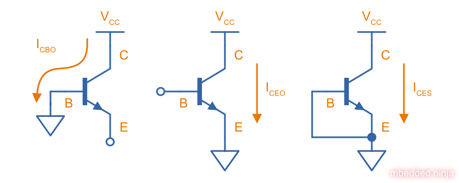
BJT Leakage Currents
BJTs do not act as perfect switches. When “off”, a small amount of leakage current will flow depending on the applied voltage to each of it’s terminals. Leakage currents for BJT are normally in the \(nA\) range. For many applications, this amount of leakage does not effect the operation in any significant way. However, for certain applications such as extremely low-power devices and low-current measurement circuits, some \(nA\) of leakage can be large enough to cause issues.
There are three main leakage parameters specified in BJT datasheets, which are explained in detail below. Most leakage currents exponentially increase with temperature.
Icbo
\(I_{cbo}\) (collector-base cut-off current) is the leakage from the collector to base with the emitter open-circuit (i.e. not connected to anything). The o stands for “open”. This essentially the leakage current of the collector-base diode with reverse bias. It is the most common leakage current value (if any) that you’ll find on a BJTs datasheet. The onsemi BC547BTF gives a \(I_{cbo,max} = 15nA \) in it’s datasheet9.
Iceo
\(I_{ceo}\) (collector-emitter cut-off current) is the leakage current from collector to emitter with the base open-circuit. JEDEC calls this the collector cut-off current, base open10. Not commonly listed on datasheets.
Ices
\(I_{ces}\) is the leakage from collector to emitter with the base connected to the emitter (the s stands for “shorted”). Not commonly listed on datasheets.
Leakage Measurement Circuits
The three leakage parameters are measured as shown in the following circuits.
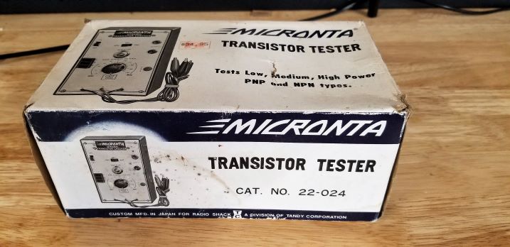
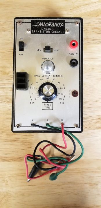
Transistor Testers
Many older handheld multimeters contain transistor testers for testing BJT transistors in the popular TO-92 through-hole package (you should see some 3 or 4 little holes on the front panel with letters similar to CBE).
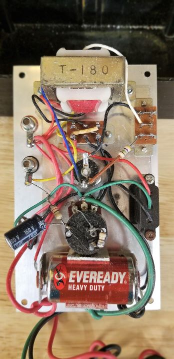
I also found this older “Micronta Transistor Tester” device on TradeMe many years ago, I bought in purely out of interest (Micronta being a brand belonging to Radio Shack):
External Resources
This is a great video on two not-so-common transistor biasing configurations.
The you are looking for a slice of history and some informative transistor information, check out the 1964 edition of the GE Transistor Manual.
References
PBS (1999). Evolution of the Transistor. Retrieved 2022-01-10, from https://www.pbs.org/transistor/background1/events/trnsevolution.html. ↩︎
Byju’s. Characteristics Of A Transistor. Retrieved 2022-08-15, from https://byjus.com/physics/characteristics-of-a-transistor/. ↩︎
Learnabout Electronics (2020, Dec 29). Learnabout Electronics - Bipolar Junction Transistors (BJTs). Retrieved 2022-08-15, from https://learnabout-electronics.org/Semiconductors/bjt_05.php. ↩︎
Wikipedia (2020, Mar 22). Hybrid-pi model. Retrieved 2022-08-14, from https://en.wikipedia.org/wiki/Hybrid-pi_model. ↩︎ ↩︎ ↩︎ ↩︎
http://www.semiconductormuseum.com/Transistors/Motorola/Haenichen/Haenichen_Page11.htm, retrieved 2021-06-20. ↩︎
Unisonic. S8050 NPN Silicon Transistor: Low Voltage High Current Small Signal NPN Transistor. Retrieved 2022-10-24, from http://www.unisonic.com.tw/datasheet/S8050.pdf. ↩︎
El-Component. S8050 Bipolar Transistor. Retrieved 2022-10-24, from https://www.el-component.com/bipolar-transistors/s8050. ↩︎
Wikipedia. Safe operating area. Retrieved 2021-08-23, from https://en.wikipedia.org/wiki/Safe_operating_area ↩︎
onsemi (formally Fairchild) (2002). BC546 / BC547 / BC548 / BC549 / BC550: NPN Epitaxial Silicon Transistor (datasheet). Retrieved 2022-10-10, from https://nz.mouser.com/datasheet/2/308/BC550_D-1802078.pdf. ↩︎
JEDEC. Dictionary: collector cutoff current, base open (ICEO). Retrieved 2022-10-10, from https://www.jedec.org/standards-documents/dictionary/terms/collector-cutoff-current-base-open-iceo. ↩︎
Authors


This work is licensed under a Creative Commons Attribution 4.0 International License .
Related Content:
- Shift Registers
- Peltiers (Thermoelectric Cooler)
- August 2015 Updates
- Electropermanent Magnets (EPMs)
- Neon Sign Transformers
Tags
- electronics
- components
- transistors
- bipolar junction transistors
- BJTs
- base
- collector
- emitter
- reverse active mode
- amplifiers
- common-emitter
- CE
- common-collector
- CC
- common-base
- CB
- grounded base
- Miller capacitance
- Widlar
- Widlar current mirror
- current mirrors
- Micronta
- Radio Shack
- transistor testers